
The importance value in SMT process when layout the SMT stencil
Author: Paul Lu
As a professional EMS foundry, to achieve customer expectations of quality, delivery and service is the purpose of our eternal pursuit of the cause. Since we founded Pronology Services Inc., we always focus on the quality and seeking for surviving and we have a good quality reputation in the customer's mind too. As we all know that the management of a factory is "success in management and win in the details", so it is no accident that quality should be achieved. Our scientific management system, a good execution ability, continuously effective correction and self-review ability are our effective management measures, again to do a good pre-preparing and confirming of each detail, then it could prevent the abnormalities from happening, to let the production movement easier to be effectively completed. Today, we are here to introduce to everyone, on the pre-preparation aspect, how do we through confirmation of the layout for SMT stencil, let the produced SMT stencils can have a better-quality performance in the SMT process.
I. The Stencil Layout process of Pronology Services (China) Inc
- 1.1 To get the customer's Gerber file, and to confirm the Panel information with Customer too.
- 1.2 To get the PCB (Bare PCB FAB)
- 1.3 SMT engineers to study customer data, and according to the Layout on the part, as well as our process
- experience, resulting in "SMT stencil layout notice"
- 1.4 Send to the "SMT stencil layout notice" to the Supplier, and notify the manufacturer to layout the
- stencil as per our notice.
- 1.5 Inspection and Storage once Stencil come back
II. What’s the purpose of "SMT stencil layout notice" achieve to
- 2.1 A reasonable Layout of each QFN grounding pad to prevent internal short
- 2.2 Reasonable choice of steel thickness, both under the guarantee of tin, but also to prevent short circuits increase
- 2.3 Appropriate to increase for the easily plug components, increase the welding strength
III. SMT stencil Layout method
- 3.1 stencil Layout design should consider the demolding of solder paste, it is determined by three factors:
- 3.1.1 Aspect ratio / Area ratio
- 3.1.2 Side of hole’s wall geometry
- 3.1.3 Hole wall smoothness
Among the three factors, the latter two factors are determined by the Supply manufacture technology, the former one we consider more. Because we has fully imported the Laser stencil, and Laser stencil has a good price and performance, so here we focus on the Laser stencil Layout design.
First of all, we know the Aspect ratio and area ratio:
Aspect Ratio: The ratio of Layout width and stencil thickness.
Area ratio: The ratio of Image area to wall cross-sectional area, as shown below:
In general, to get a good mold release effect, the aspect ratio should be greater than 1.5 and the area ratio should be greater than 0.66.
When considering the aspect ratio, when considering the area ratio? Usually, if the Layout length does not reach 5 times the width, should consider the area ratio to predict the release of solder paste, other cases consider the aspect ratio.
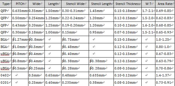
Here are some examples of Layouts for components:
Of course, the Layout of the stencil design, we can’t blindly pursue the aspect ratio or area ratio while ignoring the other process issues, such as short, insufficient solder and more.
In addition, for 0603 (1608) and above the chip components, we should think about how to prevent solder ball more.
3.2 Here we will briefly introduce the Layout of the glue process stencil (SMT template) design:
Glue because of its characteristics, the Layout design experience is very important.
Glue stencil Layout generally open a long strip or round hole;
3.2.1 Strip width W should be: 0.3mm ≤ W ≤ 2.0mm
3.2.2 The diameter of the hole is:
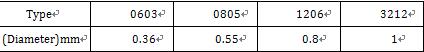
3.2.3 Indian plastic stencil thickness of the general choice of 0.15 mm ~ 0.2mm
IV. Pronology Services (China) Inc SMT Stencil Layout design tips:
- 4.1 Fine pitch IC / QFP, in order to prevent stress concentration, the best way was to let the
- Lead PAD with two rounded corners;
- 4.2 BGA and 0402, 0201 components open square hole;
- 4.3 QFN grounding pad to open the "十" shape, "十" shape from the PCB grounding PAD
- outer edge to be greater than 0.5MM blank
- 4.4 USB, Mini USB, CF / SD card, such as the ground PAD to be 1: 1. 2 length of the hole to increase the solder past;
- 4.5 Stencil design, the Layout width should ensure that at least four of the largest solder ball can smoothly through.
The above brief description, it was some usually think factors of SMT engineers to layout the stencil. We hope thought our continue carefully working and can to give our customers more satisfied with the quality and service.