DIP Process is known as dual in line package process which is the combination of electronic components and PCB assembly process in the traditional soldering technology.
The soldering technology is to insert the components through PTH of PCB by hand, then spray the flux onto the bottom side of the board by flux sprayer machine. The board after flux process goes through the wave soldering machine via pre-heating and soldering process, melted solder would be wetting on the leads and PTH of PCB for electronic components and PCB-PAD. It’s the detail of DIP process.
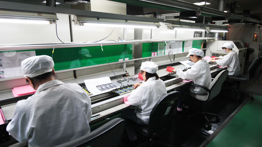
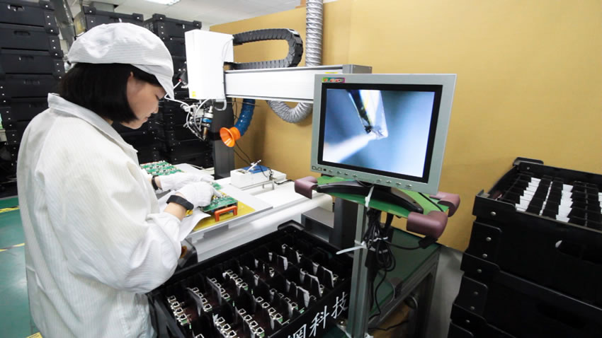
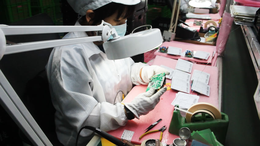
Currently, PSI have two DIP insertion lines. The detail processes are Forming work(Includes PCB de-paneled by PCBA slicer or routing machine, IC lead forming, lead cutting for vertical parts)、Manual insertion、Flux spraying、Wave soldering、Touch up(Includes small soldering pot、auto-iron soldering machine、auto DIP machine and touch up by hand)、PCBA cleaning、Post-process(Includes glue dispensing, screw driving, heat sink pasting, press fit)、100% QC visual inspection、defect board repairing and QA sampling inspection. Through well SOP and processes system with talent production operators, The semi-products goes out perfectly.
According to customer’s requirements, there is an optional process of Auto PCBA conformal coating. The detail processes are PCBA protection for screw hole and without coating area、Spaying coating by PVA machine、Tunnel bake oven、Stacked conveyor belt and 100% visual inspection by QC, and then repeat the same process for second side coating. The purpose of coating process makes PCBA insulation, Moisture-proof and Dust-proof to increase the product life.
Equipment List:Click in
Equipment image:More